Vivado Design Flows: Non-Project Mode
In this post we will generate a bitstream in Vivado using the Non-Project Mode.

In the first installment of this two-part series about the Vivado Design Flows, we discussed Vivado's Project and Non-Project Modes. We also defined the minimal set of files needed for an FPGA design and described a folder structure to store those files. Finally, we created a project using the GUI and generated the bitstream file that we can use to program our FPGA.
In the second part of this series, we will generate a bitstream file from the same design sources using the Non-Project Mode. We will accomplish this by creating a script that executes each step of the development flow.
Setting the Target Device
The first step in our non-project mode script is to set the device for which we want to generate a bitstream. We do this by using the 'set_part' command.
# Set the target device
set_part        xc7k70tfbg676-1
Reading the Input Files
The next step is to read the input files. Here we'll use three commands, one for each file type: RTL files, IP files, and constraints files.
- For the RTL files, we'll use the 'read_verilog' command (there's an equivalent 'read_vhdl' command for VHDL sources)
- For the IP files, we'll use the 'read_ip' command
- For the constraints files, we'll use the 'read_xdc' command
# Read the design files
read_verilog    ../rtl/clk_div.v
read_verilog    ../rtl/clk_gen.v
read_verilog    ../rtl/clkx_bus.v
read_verilog    ../rtl/clogb2.vh
read_verilog    ../rtl/cmd_parse.v
read_verilog    ../rtl/dac_spi.v
read_verilog    ../rtl/debouncer.v
read_verilog    ../rtl/lb_ctl.v
read_verilog    ../rtl/meta_harden.v
read_verilog    ../rtl/out_ddr_flop.v
read_verilog    ../rtl/reset_bridge.v
read_verilog    ../rtl/resp_gen.v
read_verilog    ../rtl/rst_gen.v
read_verilog    ../rtl/samp_gen.v
read_verilog    ../rtl/samp_ram.v
read_verilog    ../rtl/to_bcd.v
read_verilog    ../rtl/uart_baud_gen.v
read_verilog    ../rtl/uart_rx_ctl.v
read_verilog    ../rtl/uart_rx.v
read_verilog    ../rtl/uart_tx_ctl.v
read_verilog    ../rtl/uart_tx.v
read_verilog    ../rtl/wave_gen.v
read_ip         ../ip/char_fifo/char_fifo.xci
synth_ip        [get_ips char_fifo]
read_ip         ../ip/clk_core/clk_core.xci
synth_ip        [get_ips clk_core]
read_xdc        ../constraints/wave_gen_pins.xdc
read_xdc        ../constraints/wave_gen_timing.xdc
Synthesizing IP Cores
IP cores are usually described in a vendor-specific format that cannot be directly simulated or synthesized. Therefore, we must synthesize the IP cores using the synth_ip command, as shown in lines 25 and 27 of the script above. Vivado will find the synthesis results whenever the IP core is instantiated in our RTL sources.
Synthesizing the Design
We are now ready to synthesize our design. To run synthesis, we use the 'synth_design' command and we pass the name of the top-level unit (Verilog module or VHDL entity) in our design.
After the 'synth_design' command runs, we will have a synthesized design in memory, ready to be placed and routed. However, since we are in non-project mode, we won't automatically receive any reports about the synthesized design, and we will not be able to access the design itself after closing the Vivado session.
The 'write_checkpoint' command allows us to store the current state of the design (in this case, the synthesized design) in a single file. We can then load the design checkpoint in the Vivado GUI or the command line, and run any analysis and report tools that we'd like. We can also run those reports immediately after running synthesis and writing the design checkpoint, as shown in the code below.
# Synthesize the design and write the synthesis results
synth_design              -top wave_gen
write_checkpoint          -force ./post_synth
report_timing_summary     -file ./post_synth_timing_summary.rpt
report_power              -file ./post_synth_power.rpt
report_clock_interaction  -delay_type min_max -file ./post_synth_clock_interaction.rpt
report_high_fanout_nets   -fanout_greater_than 200 -max_nets 50 -file ./post_synth_high_fanout_nets.rpt
Placing the Design
We run placement by executing the 'place_design' command. We don't need to indicate a target for placement; Vivado will use the synthesized design from the previous step.
Though not necessary, running design optimization ('opt_design') before placement and physical optimization ('phys_opt_design') after placement usually helps reduce resource utilization and makes it easier to achieve timing closure.
# Place the design and write the placement results
opt_design
place_design
phys_opt_design
write_checkpoint      -force ./post_place
report_timing_summary -file ./post_place_timing_summary.rpt
Routing the Design
We run routing by executing the 'route_design' command. We don't need to indicate a target for the routing; Vivado will use the placed design from the previous step.
The same strategy for writing design checkpoints and generating reports applies to the routed design as well.
# Route the design and write routing results
route_design
write_checkpoint          -force ./post_route
report_timing_summary     -file ./post_route_timing_summary.rpt
report_timing             -sort_by group -max_paths 100 -path_type summary -file ./post_route_timing.rpt
report_clock_utilization  -file ./clock_util.rpt
report_utilization        -file ./post_route_util.rpt
report_power              -file ./post_route_power.rpt
report_drc                -file ./post_imp_drc.rpt
Generating the Bitstream
After our design has been routed successfully, we are finally ready to write the bitstream file that can be programmed onto our FPGA. To do this, we use the 'write_bitstream' command.
We must pass the name of the new bitstream file as an argument to the 'write_bitstream' command. The '-force' option automatically overwrites an existing bitstream file with the newly created one, a common scenario where we are making changes to our design.
# Write the bitstream
write_bitstream -force ./wavegen.bit
Running the Script
We can run the entire script at once by opening a terminal in the 'project' folder (where we have stored our non-project mode script as 'wavegen.tcl') and running Vivado in command-line mode:
vivado -mode tcl -source wavegen.tclWe can see that the bitstream file has been created, along with the design checkpoints and reports for each stage of the process.
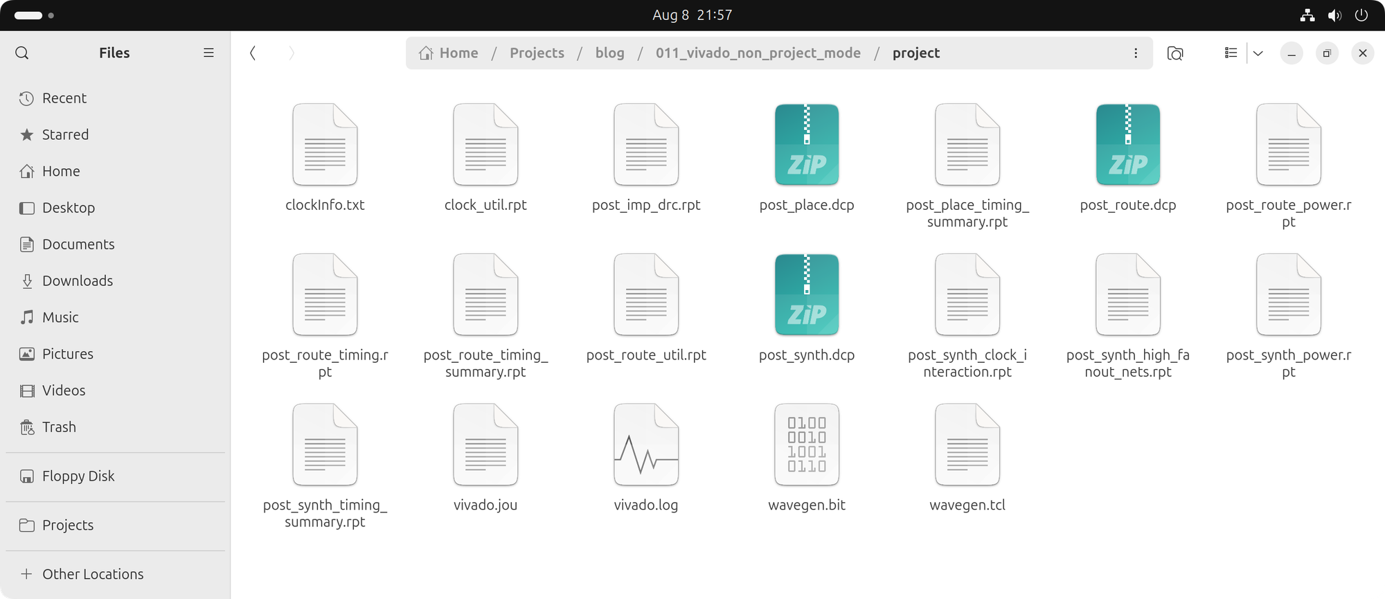
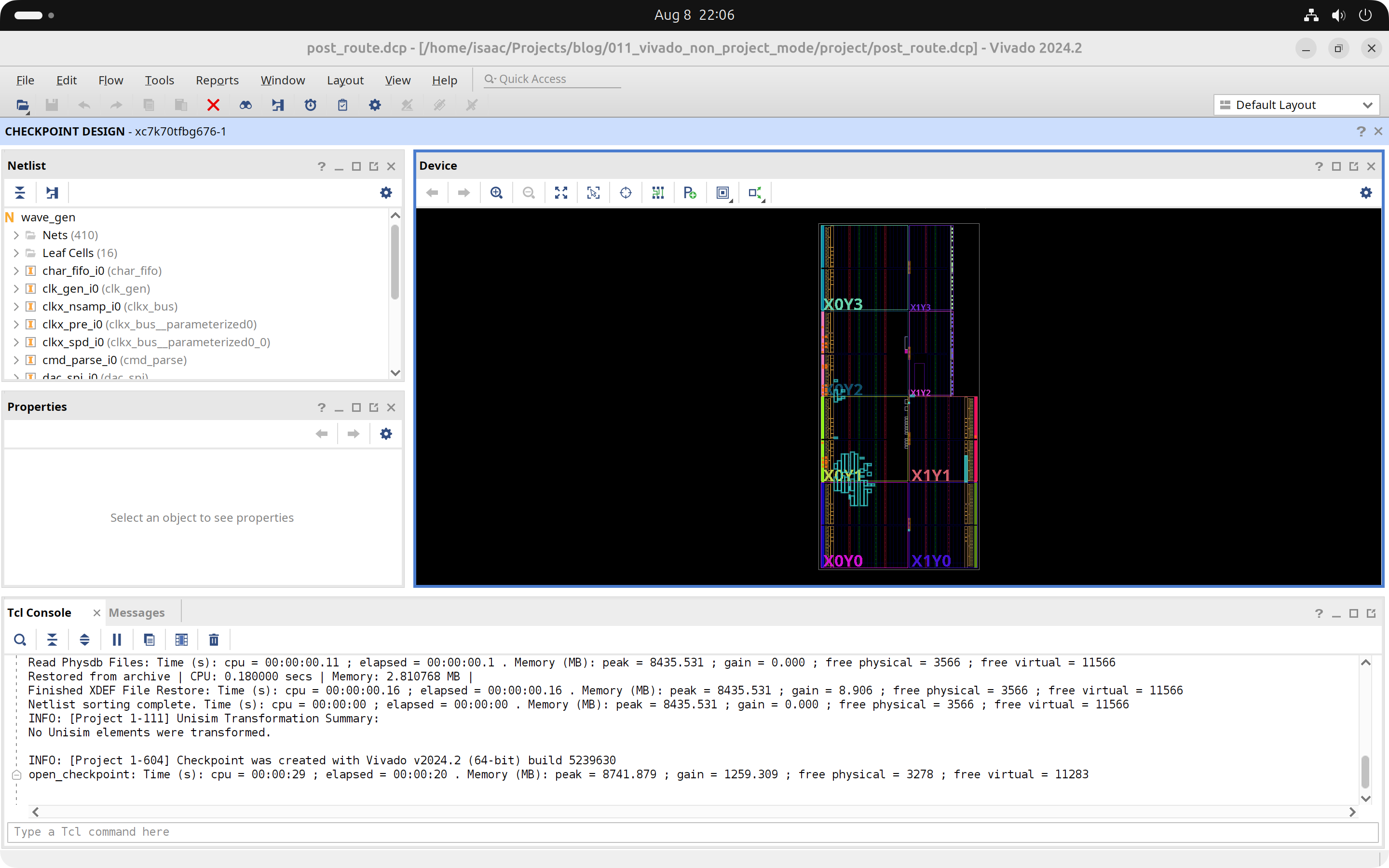
We can examine the design checkpoints by launching the Vivado GUI and selecting 'File' → 'Checkpoint' → 'Open...'. From there, we can choose one of the design checkpoint files (those with the .dcp extension) stored in the 'project' folder. Since we are in Non-Project Mode, the Vivado GUI does not display the Flow Navigator pane on the left-hand side.
Cheers,
Isaac